2026: Volume 7, Issue 1
Current Issue
 Abstract
  PDF
PDFMagnetization of Dimensional Diluted Magnetic Semiconductors
Misgana Taraka Inkosa1, Argacho Nigusa2
1SLU College of Natural Sciences, Department of Physics, Ethiopia
2SLU College of Natural Sciences, Department of Physical Chemistry, Ethiopia
*Corresponding author: Misgana Taraka Inkosa, SLU College of Natural Sciences, Department of Physics, Ethiopia, Tel: 0920665525, Email: [email protected]
Received: December 24, 2025 Published: May 22, 2026
Citation: Inkosa MT, Nigusa A. (2026). Magnetization of Dimensional Diluted Magnetic Semiconductors. Nanoparticle. 7(1):22.
Copyright: Inkosa MT and Nigusa A. © (2026).
ABSTRACT
The one dimension, two dimension and the three dimension relation in case of concentration and temperature versus reduced magnetization have been over looked. Recently information technology is one of the important issues for the optical, electrical and magnetic properties of diluted magnetic semiconductors. One of the most useful aspects of semiconductors resides in their capacity to be doped with impurities, by which the electrical properties can be tuned be interpreted as a function of temperature and magnon concentration. DMs is of fundamental interest and may enable future spin-optoelectronic devices. In order to enable to them useful for such devices efforts have been made to develop diluted magnetic semiconductors (DMS) in which small quantity of magnetic ion is introduced in to normal semiconductors. ZnMnTe with face centered cubic structure and long-range antiferromagnetic ordering is study within the frame work of the Heisenberg model. The Hamiltonian includes exchange interactions with the nearest neighbors and Zeeman terms.
Keywords: Diluted Magnetic Semiconductors, Low Dimensional, Antiferromagnetic
INTRODUCTION
Information technology is one of the important issues in the 21st century. Developing alternative high speed and low energy consuming information technology is urgently needed [1]. The mass, charge, and spin of electrons in the solid state lay the foundation of the information technology we use today. Semiconductor devices generally take advantage of the charge of electrons, whereas magnetic materials are used for recording information involving electron spin. If both the charge and spin of electrons can be used to further enhance the performance of devices, so called spintronics, we may then be able to use the capability of mass storage and processing of information at the same time, thus leading to a brand new era of information technology [2,3,4-7].
DMS bridge the physics of semiconductors and magnetic since they show typical semiconductor behavior and they also reveal pronounced magnetic properties. Diluted magnetic semiconductors (DMS) in which the semiconductor cations are partially substituted by magnetic elements, is one of the important materials for the realization of spintronics. The rapid progress achieved in DMS technologies which use non-equilibrium growth methods, such as molecular beam epitaxy (MBE) the ferromagnetic transition was observed in II-VI, III-V and IV-VI semiconductor compounds. In most studied DMS manganese is used as a magnetic impurity. Manganese doped II-VI and IV-VI DMS mostly exhibit antiferromagnetism, spin glasses and paramagnetism, but they also show ferromagnetic transition at low temperatures.
The ability to synthesize DMS in low dimensional nanostructures could provide new building blocks for spintronics as well as open up new opportunities for fundamental physical studies [2,3]. Solid state magnetism and semiconductor physics are two of the most important areas of current research in condensed matter physics [4,6,8,9].
A semiconductor is typically smaller than  (i.e. small energy gap) and room-temperature thermal energy or excitation from visible-light photons can give electrons enough energy for "jumping" from the valence into the conduction band. The energy gaps of some semiconductors are listed in Table 1.1. the small energy gap in semiconductor determines among other things the wavelengths of light that can be absorbed or emitted by the semiconductors.
Table 1: The energy gap of the most common semiconductors [18].
|
Semiconductor |
Energy gap ( |
|
Germanium |
0.67 |
|
Gallium arsenide |
1.42 |
|
Cadmium selanide |
1.74 |
|
Indium arsenide |
0.46 |


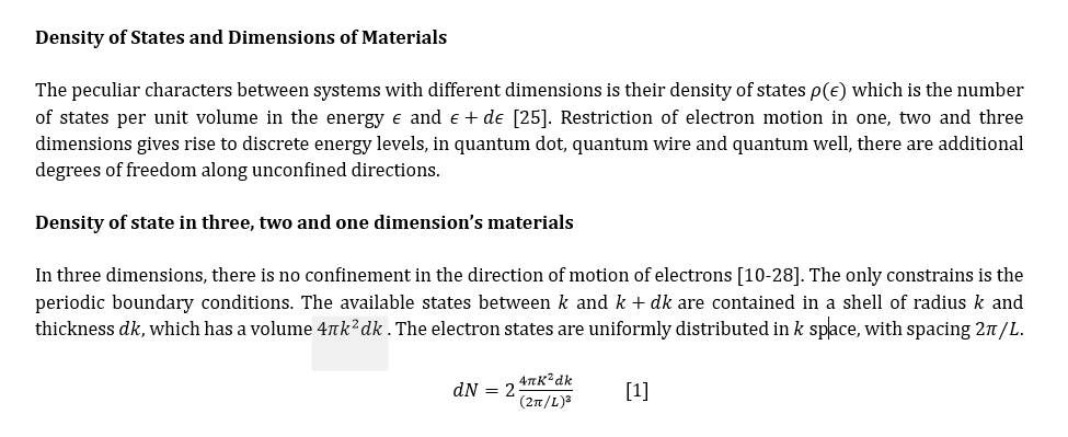
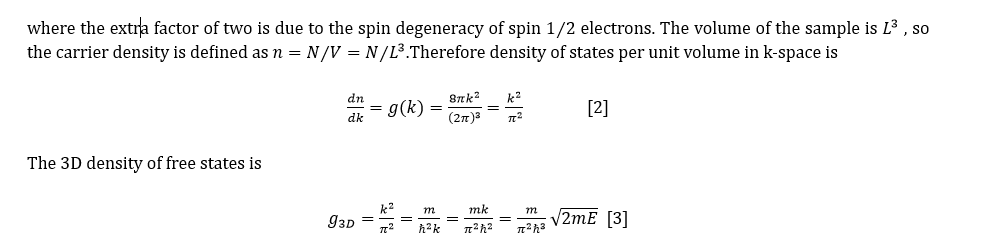
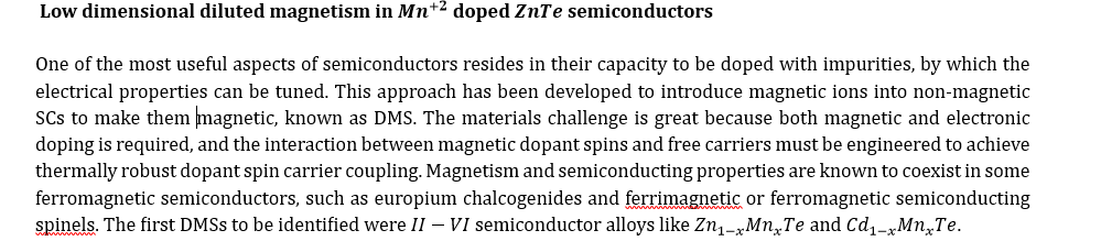
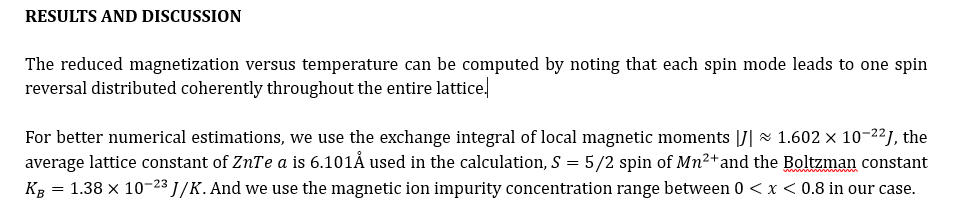
The above equation tells that the density of states in 3D is square root dependent on energy. It is known that the unconfined wave functions within 3D box are plane waves in all three dimensions.
In quantum wells, the electrons motion is confined into two dimensions and unconfined in the other dimensions; let assume its motion in the z-direction. Thus, the total energy of the system is the sum of the energy along the quantized direction and the energy along the other two directions [29].
Magnetic materials
In order to understand why semiconductors are traditionally not magnetic and how it is possible to introduce magnetic behavior in these materials is first necessary to look at the fundamental origins of magnetic behavior. And then analyze how magnetic behavior can be exploited in the development of dilute magnetic semiconductor compounds. Magnetism in materials arises from the fundamental property of electron spin, which is the intrinsic angular momentum of an electron.
.png)
Figure 1: Reduced magnetization versus temperature in 2D and 1D.
The aim in this subsection is to investigate the antiferromagnetic Heisenberg model spin system consisting of two interpenetrating sublattices and, which is described by the Hamiltonian
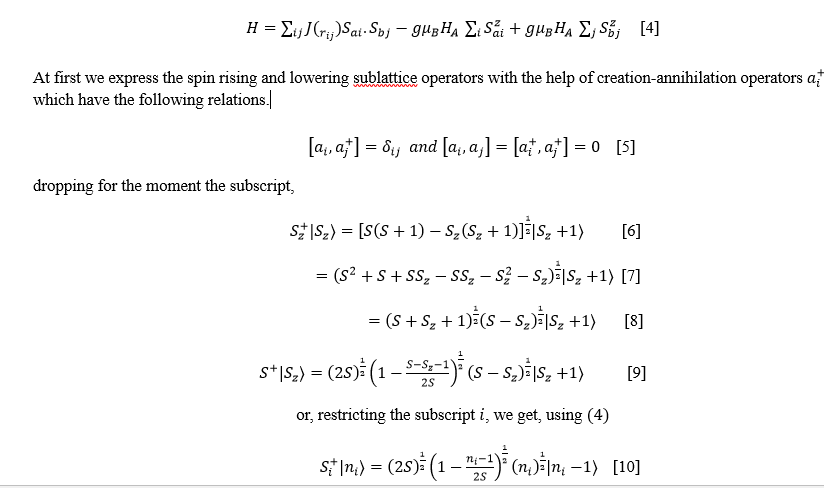
.png)
Figure 2: Reduced magnetization versus temperature in 3D
.png)
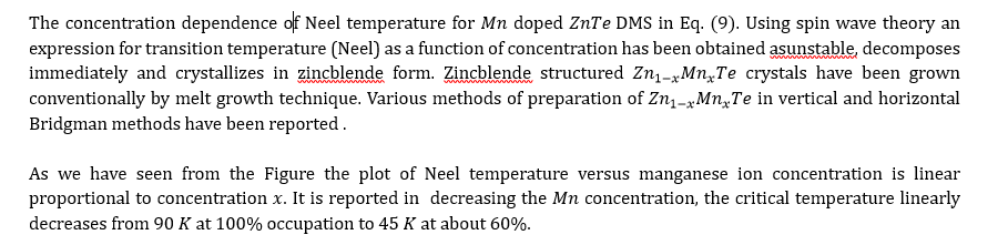
Figure 3: Neel temperature versus Mn2+ concentration in 1D, 2D, 3D

In a few past decades, the hurriedly growing field of diluted magnetic semiconductors has attracted interest to their potential for spintronics devices mean that they have both semiconducting and magnetic properties which provide the possibility to manipulate electron charge and spin at the same time and opens a new field in semiconductor technology. DMSs are known by their special property like addition of magnetic impurities instead of few portions of compound semiconductors at cation sites. Advances in semiconductor materials technology has resulted in the development of a wide range of electronic and optoelectronic device structures with extremely small dimensions. Over the last decades the field of dilute magnetic semiconductors (DMS) has seen important developments both in fundamental aspects and prospective technological applications. From the point of view of prospective applications, the marriage between the world of low dimensional semiconductors.
CONCLUSION
This article is concluded as the impurity or the concentration is increased the temperature,the heat capacity and magnetization(magnetic property) of the diluted semiconductor is/are affected.In three dimensions, there is no confinement in the direction of motion of electrons. The only constrains is the periodic boundary conditions.The result matches with experimental values described for Neel temperature for increases when the concentration of manganese ion increases in the given range. Diluted Magnetic Semiconductors are known by their special property like addition of magnetic impurities instead of few portions of compound semiconductors at cation sites. Advances in semiconductor materials technology has resulted in the development of a wide range of electronic and optoelectronic device structures with extremely small dimensions.
REFERENCES
- Li X, Yang J. (2016). First-principles design of spintronics materials. National Science Review, 3(3):365-381.
- A. Twardowski. Magnestism of Semimagnetic Semiconductors. (1991). Physica Scripta. T 39, 124.
- Liu J. (2006). Diluted Magnetic Semiconductor Nanomaterials Fabrication by a Chemical Vapor Deposition Method. University of New Orleans Theses and Dissertations. 426.
- Read DE. (2001). Electrical and magnetic properties of n_(-c) d(_(-1-x))〖Mn(〗_(-x))Te close to the metal-insulator transition(Doctoral dissertation, Durham University).
- Averous M, Balkanski M. (1991). Semimagnetic semiconductors and Diluted magnetic Semiconductors (Plenum press, New York, first edition, p.84-99.
- Lindberg S. Fabrication and characterization of Mg-Ni hydride thin films for photovoltaic applications.
- Greve DW. (2012). Semiconductor device technology. Department of Electrical and Computer Engineering, Carnegie Mellon University.
- Singh R. (2015). Excitations in Semiconductor Quantum Wells Studied Using Two-Dimensional Coherent Spectroscopy, (Doctoral dissertation, University of Colorado at Boulder).
- Sze SM. (2002). Semiconductor devices, physics and technology 2nd ed. New York: John Wiley & Sons Inc, p. 18.
- Kittel C. (2005). Introduction to solid state physics. 8th Ed. (John Wiley and Sons, USA.).
- Srivastava JP. (2009). Elements of solid state physics, 2ndedition, (PHI PL. New Delhi-11001).
- Chua LL Zaumseil J, Chang JF, Ou E.C.W, Peter KH Ho, Sirringhaus H, Friend RH. (2005). General observation of n-type field-effect behaviour in organic semiconductors. Nature. 434(7030): 194,
- Ashkroft NW, Mermin ND. (1976). Solid State Physics, (Harcourt collage publishers, USA,)
- Angus R. (2008). The Materials Science of Semiconductors. New York, USA: Springer, p. 40,
- Green EDH. (2014). Temperature Dependence of Semiconductor Conductivity,
- Shaheen A, Zia. W, Anwar. MS. (2011). Band structure and electrical conductivity in semiconductors, LUMS School of Science and Engineering, Lahore, Pakistan.
- Zeghbroeck B. (2004). Principles of semiconductor devices. Colorado University, 34.
- Colinge JP, Colinge CA. Physics of Semiconductor Devices (Kluwer Academic Publishers, 2002), p.17, 34.
- Reimann SM, Manninen M. (2002). Electronic structure of quantum dots. Reviews of Modern Physics. 74(4):1283.
- Grabert H, Devoret M.H. eds. ( 2013) Single charge tunneling: Coulomb blockade phenomena in nanostructures (Vol. 294). Springer Science & Business Media.
- Kumar S, Nann T. (2006). Shape control of II-VI semiconductor nanomaterials. Small. 2(3):316-329.
- Balaguru RJB, Jeyaprakash BG, Introduction to Materials and Classification of Low Dimensional Materials. Hung. N, Thermoelectric properties of low dimensional semiconductors, (Doctoral dissertation, MS thesis), 2016.
- Cohen-Tannoudji C, Guéry-Odelin D. (2011). Advances in atomic physics: an overview.
- Nouredine Zittile. (2009). Quantum Mechanics Concepts and Application (2nd ed), Jhon Willey and Sons, Ltd.
- Mathieu R. (2002). Magnetism of manganites, semiconductors and spin glasses (Doctoral dissertation, Acta Universitatis Upsaliensis).
- Blugel S. (2007). Electronic Structure of Matter: Reduced Dimensions. lecture manuscripts of the spring school of the institute of solid state research.
- Wiley-VCH Verlag GmbH & Co. KGaA. (2018). Published by Wiley-VCH Verlag GmbH & Co. KGaA. Synthesis and Applications of Inorganic Nanostructures, First Edition. Huaqiang Cao.©.
- Chan WCW, Nie S. (1998). Quantum dot bioconjugates for ultrasensitive nonisotopic detection. 281(5385):2016-2018.
